Aloe vera的問題,透過圖書和論文來找解法和答案更準確安心。 我們找到下列包括價格和評價等資訊懶人包
Aloe vera的問題,我們搜遍了碩博士論文和台灣出版的書籍,推薦OwainMckimm,ZacharyFillingham,RichardLuhrs,李惠君,鍾震亞寫的 學測英文克漏字滿分攻略:綜合測驗+文意選填+篇章結構50回全真模擬題(菊8K) 和JonathanDrori的 環遊世界八十種植物都 可以從中找到所需的評價。
另外網站Lifeplan Aloe Vera Gel 200ml - Boots也說明:Life Plan Organic Aloe Vera Gel may be applied to: Dry skin conditions; Sunburn and minor burns; Stretch marks ...
這兩本書分別來自寂天 和天培所出版 。
元智大學 化學工程與材料科學學系 孫安正所指導 柯利雅的 磁性奈米顆粒擔載刺蝟路徑抑制藥物對肝癌細胞的熱療與標靶研究 (2021),提出Aloe vera關鍵因素是什麼,來自於化學合成、綠色合成、磁性奈米粒子、奈米肥粒鐵、生物醫學。
而第二篇論文長庚大學 電子工程學系 賴朝松所指導 Mamina Sahoo的 基於石墨烯及生物碳基材料的可撓式電晶體應用與能量攫取 (2021),提出因為有 石墨烯、氟化石墨烯、太阳能电池、摩擦纳米发电机、生物碳、能量收集器的重點而找出了 Aloe vera的解答。
最後網站Aloe Vera Gel - CVS則補充:Shop the best aloe vera gel products here at CVS! Learn more about the benefits aloe vera gel such as moisturizing, sunburn relief, and more for all skin ...
學測英文克漏字滿分攻略:綜合測驗+文意選填+篇章結構50回全真模擬題(菊8K)

為了解決Aloe vera 的問題,作者OwainMckimm,ZacharyFillingham,RichardLuhrs,李惠君,鍾震亞 這樣論述:
出題文章涵蓋108課綱跨領域學科的多元主題出題趨勢! 習題最豐富、命題內容與編排最接近大考的克漏字參考書! 「200篇克漏字+詳解」幫助完全掌握大考精要! 依108課綱以及111學年度起學測英文考科出題準則,由中外師合力精心編寫50回共200篇學測克漏字模擬試題,每回包含2篇綜合測驗、1篇文意選填、1篇篇章結構共200篇題組,幫助學生掌握大考題型,迅速累積大考實力! 本書特色 1. 中外專業作者及高中名師通力合著 集結多位外籍作者撰寫200篇原創文章,用字遣詞道地,文章簡潔精練,再由名校資深專業英文老師根據多年豐富教學經驗出題,同時解析考點,提點文法要項
與陷阱。兼顧閱讀文章學習及模擬考試的雙重精要,不因單純為準備考試而閱讀不道地的文章;也不因考題不佳而失準於大考方向。 2. 文章涵蓋108課綱跨領域學科的多元主題出題趨勢 選文符合108課綱及大考主題多元的出題方向,涵蓋商業、健康、文化、教育、地理、環境、娛樂等20多種主題,囊括生活化、具實用性、或較抽象專門的各式主題與題材。大量閱讀各類文章有助學生累積多樣的豐富知識,營造充實愉悅的閱讀經驗,更能訓練應試手感而臨場不畏! 3. 符合大考設計的考題練習 文章長度與所用單字皆依學測程度撰寫,內文也依「大考克漏字出題原則」規劃,如綜合測驗部分每一篇的句數約在10–15句、同
句不挖兩個洞,嚴格要求不同詞性平均出題,選項一定為高頻率單字等,完全貼切大考出題。 4. 考題解析採教學式詞彙、句構、文法、語意邏輯理解 考題解析由經驗豐富的英文老師撰寫,提供符合大考命題設計的考題練習與文法解析,協助提升考生對英文文法與句構的整體概念,在沒有老師從旁協助的狀況下也能輕鬆自我學習。 5. 「五大必考重點」提點必考要項及解題步驟 特別整理歸結歷屆考題出題方式,編寫必考重點,並搭配考古題為範例,提供解題步驟及技巧,鞏固讀者文法基礎,整理零碎的片段知識,建立有系統的語言概念。 6. 試題+解析雙書版設計,方便對照與檢討 試題本: 開數、排版皆仿真大
考試卷設計,每回測驗以實際大考綜合測驗、文意選填、篇章結構分量比重設計,以跨頁的方式呈現,創造臨場感,讓學生能模擬並掌握臨場時的時間分配,適合模考。 解析本: 詳盡的破題解析先提出考點,再簡要點明出題方向,提供答題訣竅,以快速掌握大考解題祕訣,大幅提升英文實力。 每篇文章亦有中文翻譯與關鍵英單,供考生參考、背誦。
Aloe vera進入發燒排行的影片
ミルクスライムさんの「アローナマンゴー」
This is Milk Slime's "Arona Mango".
#milkslime #ミルクスライム
───────────────────
0:00 〜 OP
0:30 〜 本編開始 (with BGM)
the beginning of the main part
1:13 〜 触り始め
begin to touch
1:17 〜 end of BGM
1:28 〜 容器から出す
take out of a container
1:35 〜 片手で触る
touch with one hand
2:00 〜 両手でガッツリ遊ぶ
play with both hands
5:00 〜 もこもこにして容器に還元
fluff up and return to the container
5:05 〜 もこもこ
fluffy
───────────────────
【テロップ書き起こし】
こちらはおまけで頂いたスライムちゃんです♪
This is a slime that was given as a present♪
色味が最高に可愛いです♡
The color is super cute ♡
キラキラの振りかけを飾っていきます!
Sprinkle shining holograms!
可愛いヒトデのチャームです
It ’s a cute starfish charm.
昼間にライトアップをしても綺麗に映えました!
It was beautiful even if it was light up in the daytime!
こちらアロエベラを含んだちゅるちゅるクリアスライムです
This is a clear slime containing aloe vera.
びっくりするくらい手に付かなくて片手で遊びやすい!
It's surprisingly easy to peel off from hands and super holdable!
半透明でトロッとした質感です♡
It is a translucent and oozy texture♡
まだ硬めなのでもちもち感もあって最高です
It's still a little stiff, so it's also very chewy.
モッチモチ故に、タッピングも楽しいです
Tapping is also fun because it is chewy.
膜が分厚くてバブル音がとっても大きいです
The film is thick and the bubble sound is loud.
今はパテ風ですが、少し溶けるとトロトロになります
It's like putty now, but when it melts a little, it becomes oozy.
ずっと揉んで遊んでられます
I was playing endlessly.
机との相性もとっても良い感じです
It goes well with table play.
音が気持ちが良すぎる〜〜!
The sound feels sooooooo good ~~!
空気を含んでもベタつかないです!
It is not sticky even if it contains air!
二倍以上に膨らみます!
It swells more than twice!
空気を含むと弾力が強くなりました!
The elasticity became stronger when it contained air!
癒し……
Healing……
マンゴーやパイナップルのトロピカルな感じの香りでした!
It had a tropical scent of mango and pineapple!
ミルクさん、素敵なスライムありがとうございました!
Thank you Milk Slime for the wonderful slime!
ごちそうさまでした!
Thank you for the meal!lol
ご視聴ありがとうございました!
Thank you for watching!!!!
───────────────────
サブチャンネル【もちよの研究室】はコチラ!
↓ ↓ ↓ ↓ ↓ ↓ ↓ ↓ ↓ ↓ ↓ ↓
https://www.youtube.com/channel/UCWmSQDBSNQTX6kpFm6lYLnw
Instagram・ twitter・Tiktok・BASE shop・メルカリはこちら!
↓ ↓ ↓ ↓ ↓ ↓ ↓ ↓ ↓ ↓ ↓ ↓
https://linktr.ee/mochiyoslimestore
スライムの提供についてはコチラ!
↓ ↓ ↓ ↓ ↓ ↓ ↓ ↓ ↓ ↓ ↓ ↓ https://www.instagram.com/s/aGlnaGxpZ2h0OjE3ODQ4ODU4NzU3MDI2MzA3?igshid=1hr3jy34zfnpo&story_media_id=2286885986591781571
イヤフォンやヘッドフォンをして聴いて頂くとよりいい音で楽しめるかとおもいますので、是非に😎
また、画面右上のチョンチョンチョンのとこから画質を1080pに設定して動画を見ていただけると、高画質でお楽しみ頂けます💪💪
───────────────────
どうもこんびんは!
もちよすらいむです🧜🏻♀️
素敵なスライマーさんのスライムのレビューや、自分で作ったスライムの動画などのASMRを中心に、いろいろなジャンルの動画を上げていきたいと思います!
【ごめんちゃいズ】
*更新が突然途絶える可能性があります🙇♀️
*慢性鼻炎でして、呼吸音が入ってしまうことがあります🤦♀️
*机に爪がコツンと当たる音が入ってしまうことがあります🙇♀️
*実家暮らしなので、稀に家族の出す生活音が紛れ込んでしまいます🙇♀️
動画を見てくださりありがとうございます💕
是非チャンネル登録をして、これからももちよの動画をお楽しみください💁♀️
───────────────────
#もちよすらいむ #mochiyoslime #べらちゃんのslimeしばき部屋 #slime #asmr #asmrsounds #asmrslime #スライム #音フェチ #音フェチ動画 #音フェチスライム #clayslime #slayslime #butterslime #cloudcream #thickslime #thickie #thickieslime #fluffyslime #clearslime #slusheeslime #slushieslime #fishbowlslime #crunchyslime #slimejapan #スライムジャパン #sakuraslime #さくらスライム #aisu屋さん #tiaslime #slimeogproof #ogslimeproof #aobaslime #awesomeslimeproof #awesomeslime #slimefantasies #slimefantasiesproof
#rodemslime #rodemslimeproof #mooncottonslime #slimebyktmproof
磁性奈米顆粒擔載刺蝟路徑抑制藥物對肝癌細胞的熱療與標靶研究
為了解決Aloe vera 的問題,作者柯利雅 這樣論述:
磁性奈米粒子在生物技術中由於擁有很多具有潛力的應用而備受關注,並且已經發展出許多的合成方法來製作磁性奈米粒子。其中化學合成法一直是該領域的重點,因為此方法能夠控制奈米粒子的尺寸、形狀、組成以及表面的特性。為了能夠把磁性奈米粒子應用於生醫上,其中一個首要條件是製作出在正常的生理狀況下的水溶液介質中可分散且穩定的奈米粒子。然而,大多數化學合成的奈米材料因為其製作成本昂貴且對環境威脅高,因此所製作出來的奈米粒子也有可能對於病人會有潛在地毒性風險。相對地,事實證明使用天然性的材料能夠有更好的生物相容性以及較低的環境毒性。儘管已經開發出多種天然奈米粒子,但是想要製作出具有可再現性的品質
、高產率以及低成本的天然奈米粒子之製造技術仍然是一大挑戰。因此本次的研究將著重於使用化學及綠色合成法且能夠得到尺寸統一、分散以及穩定的磁性奈米粒子。並且使用傅里葉轉換紅外光譜(FT-IR)、X射線繞射儀(XRD)、掃描式電子顯微鏡(SEM)、穿透式電子顯微鏡(TEM)、動態光散射粒徑分析儀(DLS)、X射線光電子能譜儀(XPS)、振動樣品磁性量測儀(VSM)分析氧化鐵奈米粒子的表面形貌及化學結構。 對於化學合成法的磁性奈米粒子,研究出一種改良的溶劑熱合成法。探討改變不同參數對磁性奈米粒子的影響例如:鐵的來源、PSSMA的含量、去離子水的量和氫氧化鈉的量。結果指出,想要得到純鐵相需
要適量的水。PSSMA可以使合成後的磁性奈米粒子穩定從而抑制晶粒成長以及預防團聚。再者,還可以調控粒徑在120 - 220 nm之間。所有合成出的磁性奈米粒子在室溫中還會擁有超順磁的性質。在最佳條件則是附著在碳量子點上,而且結合後還顯現出良好的螢光特性。還進行了細胞增殖試驗,並發現具有生物相容性。此研究的第二部分,則是研究另一種方法,綠色合成法,使用了蘆薈來製造奈米粒子及其性質之研究。並且合成了其他的磁性奈米粒子,包含鈷和鎳。在XRD中分析出磁性奈米粒子的平均直徑在8 - 30 nm,而且有很好的結晶性。從SEM中看出明顯的球形結構,從TEM中看出 Fe3O4 顆粒較大、CoFe2O4 和 N
iFe2O4 顆粒較小。另外在SEM以及TEM中得到的尺寸和XRD計算的晶粒尺寸一致。每個奈米粒子的化學特性也證實合成都是成功的。並且磁性奈米粒子也顯示出生物可相容性及無毒性。為了更好地利用磁性納米粒子進行癌症治療,表面官能基化對於降低健康組織的細胞毒性、延長循環時間、專一性靶向癌細胞以及管控藥物傳遞的療法等因素至關重要。因此在第三部分,把合成的磁性奈米粒子成功地被PEG高分子包覆。選擇包覆PEG是為了防止蛋白質吸附,從而改善循環時間並最大限度地減少宿主對奈米顆粒的反應。最後,將被PEG包覆的磁性納米粒子與 Hedgehog Pathway Inhibitors drugs結合併在體內進行測試
。有趣的是,在藥物交聯後,觀察到癌細胞的活力急劇下降。共軛焦顯微鏡也用於觀察細胞與磁性奈米載體結合過程中的反應。從結果可以證實,隨著奈米載體濃度的增加,會誘導細胞凋亡。 有了Hh 信號通路與磁性納米粒子的卓越特性相結合後,將為研究成果轉化為新穎、更好、更安全的抗癌療法。
環遊世界八十種植物
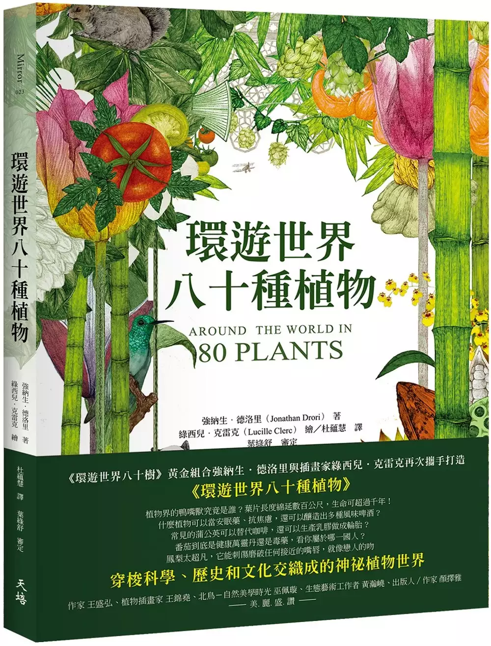
為了解決Aloe vera 的問題,作者JonathanDrori 這樣論述:
我們的世界充滿各式各樣的植物,有些美麗而奇特,有些低調而不起眼。 然而它們蘊藏的祕密和故事,都與我們的生命、生活息息相關。 這次,讓我們更靠近一點…… 植物界的鴨嘴獸究竟是誰?葉片長度綿延數百公尺,生命可超過千年! 什麼植物可以當安眠藥、抗焦慮,還可以釀造出多種風味啤酒? 常見的蒲公英可以替代咖啡,還可以生產乳膠做成輪胎? 番茄到底是健康萬靈丹還是毒藥,看你屬於哪一國人? 鳳梨太超凡,它能刺傷磨破任何接近的嘴唇,就像戀人的吻 繼《環遊世界八十樹》之後,強納生.德洛里與插畫家綠西兒.克雷克再度聯手打造第二彈《環遊世界八十種植物》
。 書寫的主題擴及到樹之外的其他植物物種,從令人嘖嘖稱奇的大王花,名稱奇特的「愛、謊言與流血」,珍貴的鬱金香、番紅花,到路邊不起眼的蒲公英,或者與日常生活有關的苧麻,可食用的海帶、番茄、大豆等等,還有利用分解、欺騙,甚至引誘、殺死之後將獵物消化殆盡的植物,或怪誕或美麗,或滋養生命或可能毒害致死,植物的世界千奇百怪,令人大開眼界。 各式各樣的植物生意盎然的存在於這個星球的許多角落,因為與人類產生了連結,而有許多故事,植物科學令人著迷,但是當它和人類歷史及文化交織在一起時又格外充滿活力。這本書裡大部分的故事揭示了人們對植物的所作所為,讓讀者看見人與植物之間緊密的連結
與相互影響,往往比我們所認知的還要深切。同時,也探討未來人類如何重新認識並珍視植物,與植物永久共生。 本書特色 ★ 全書圖文並茂,精彩細緻的插畫表現出植物自然之美,豐富視覺饗宴。 得獎記錄 水石書店(Waterstones)年度最佳選書決選(Book of the Year 2021 Shortlist) 推薦人 作家 王盛弘、植物插畫家 王錦堯、北鳥-自然美學時光 巫佩璇、生態藝術工作者 黃瀚嶢、出版人/作家 顏擇雅 美麗盛讚 媒體好評 德洛里如同一名專業的導遊,提供了許多趣聞,甚至是值得
注意的平凡普通的小細節……不論你是坐在椅子上閱讀本書中的所有內容,或者每天睡前在床上翻閱一頁,德洛里巧妙設計的這趟旅程,都值得我們跟隨其後。──《自然史雜誌》(Natural History Magazine) 因為插畫家綠西兒.克雷克生花妙筆讓圖像栩栩如生,《環遊世界八十種植物》成為一趟美麗而鮮豔的植物之旅。──《環境雜誌》(The Environmental Magazine) 這本令人屏息的書是份珍貴寶物,充滿趣味的知識與色彩豐富的插畫,都會讓你不自覺的迷失其中。──Greatlist 帶領讀者進入一段橫跨我們星球的旅程,一路上
讓我們停下來嗅聞花朵,以及欣賞各式各樣的物種。──《史密森尼》(Smithsonian Magazine) 在這本書中,對於植物訊息充分的描述,展現迷人的、廣博的、具教育性,以及美學的愉悅,讀者透過反覆的觀察與驚嘆,將會認識更多植物。──《書單》(Booklist)
基於石墨烯及生物碳基材料的可撓式電晶體應用與能量攫取
為了解決Aloe vera 的問題,作者Mamina Sahoo 這樣論述:
Table of ContentsAbstract.......................................................................................................iFigure Captions........................................................................................xiTable Captions...................................................
....................................xxiChapter 1: Introduction1.1 Flexible electronics................................................................................11.2 Graphene the magical material ………………………….……….......21.2.1 Synthesis of graphene…………………………….….…...21.2.1.1 Mechanical exfoliati
on of graphene………………...……21.2.1.2 Epitaxial growth on Sic substrate………………….…..31.2.1.3 Chemical vapor deposition (CVD) method………….…..41.2.2 Graphene transfer…………………………………………....41.3 Application of graphene based Electronics……………………….......51.3.1 Graphene based flexible transparent electrode
……………….61.3.2 Top gated Graphene field effect transistor…………………….71.4 Challenges of flexible graphene based field effect transistors.……….91.5 Energy harvesting devices for flexible electronics………….........….91.6 Solar cell…………………………………………………………...101.6.1 Device architecture…………………………………………101.
6.2 Issues and Challenges of Perovskite solar cells………...121.7 Triboelectric nanogenerator (TENG)………………………………121.7.1 Working mode of TENG………………………………….141.8 Applications of TENG………………………………………………151.8.1 Applications of graphene based TENG…………………....151.8.2 Applications of bio-waste material ba
sed TENG………….171.9 Key challenges of triboelectric nanogenerator…………………....…191.10 Objective and scope of this study………………………………....19Chapter 2: Flexible graphene field effect transistor with fluorinated graphene as gate dielectric2.1 Introduction………………………………………………………....212.2 Material preparation a
nd Device fabrication………………. 232.2.1CVD Growth of Graphene on Copper Foil………………….232.2.2 Transfer of graphene over PET substrate……………...........252.2.3 Fabrication of fluorinated graphene ……………...........252.2.4 F-GFETs with FG as gate dielectric device fabrication……262.2.5 Material and electrical C
haracterization …………………272.3 Results and discussion…………………………………………….282.3.1 Material characterization of PG and FG……………...…...….282.3.2 Electrical characterization of F-GFET with FG as dielectrics..332.3.3 Mechanical stability test of F-GFET with FG as dielectrics ….362.4 Summary…………………………………………………
………....40Chapter 3: Robust sandwiched fluorinated graphene for highly reliable flexible electronics3.1 Introduction………………………………………………………….423.2 Material preparation and Device fabrication ………………….........443.2.1 CVD Growth of Graphene on Copper Foil…………………...443.2.2 Graphene fluorination …...…….…………
…………..............443.2.3 F-GFETs with sandwiched FG device fabrication....................443.2.4 Material and electrical Characterization…..............................453.3 Results and discussion ……………………………………...............453.3.1 Material characterization of sandwiched…………………….453.3.2 Electric
al characterization of F-GFET with sandwiched FG....473.3.3 Mechanical stability test of F-GFET with sandwiched FG…503.3.4 Strain transfer mechanism of sandwiched FG………………513.4 Summary…………………………………………………………....53Chapter 4: Functionalized fluorinated graphene as a novel hole transporting layer for ef
ficient inverted perovskite solar cells4.1 Introduction………………………………………………………….544.2 Material preparation and Device fabrication......................................564.2.1 Materials ………………………...…………………………564.2.2 CVD-Graphene growth ……………………………...…...564.2.3 Graphene fluorination …………………………………….564.
2.4 Transfer of fluorinated graphene…………………………...574.2.5 Device fabrication …………………………………….….574.2.6 Material and electrical Characterization …….....................584.3 Results and discussion …………………………………………….594.3.1 Surface electronic and optical properties of FGr……….….594.3.2 Characterization o
f FGr and perovskite surface ……….…644.3.3 Electrical performance of PSC………………….…….…...694.3.4 Electrical performance of Flexible PSC……………………724.4 Summary…………………………………………………………...78Chapter 5: Flexible layered-graphene charge modulation for highly stable triboelectric nanogenerator5.1 Introduction…………
…………………………………………....795.2 Experimental Section……………………………………………….825.2.1 Large-area graphene growth ……………………………….825.2.2 Fabrication of Al2O3 as the CTL …………………………...825.2.3 Fabrication of a Gr-TENG with Al2O3 as the CTL………825.2.4 Material characterization and electrical measurements…….835.3 Results
and discussion.…………………………………...…………845.3.1 Material Characterization of Graphene Layers/Al2O3……845.3.2 Working Mechanism of Gr-TENG with Al2O3 as CTL…915.3.3 Electrical Characterization of Gr-TENG with Al2O3 CTL…945.3.4 Applications of the Gr-TENG with Al2O3 as CTL……….1015.4 Summary…………………………………………
……………….103Chapter 6: Eco-friendly Spent coffee ground bio-TENG for high performance flexible energy harvester6.1 Introduction…………………………………………………….......1046.2 Experimental Section…………………………………………….1086.2.1 Material Preparation …………………………………….1086.2.2 Fabrication of SCG powder based TENG………………...1086
.2.3 Fabrication of SCG thin-film based TENG ………………1096.2.4 Material characterization and electrical measurements….1106.3 Results and discussion.…………………………………...………1116.3.1 Material Characterization of SCG powder and thin film….1116.3.2 Working Mechanism of SCG-TENG……………………...1186.3.3 Electrical Cha
racterization of SCG-TENG……………….1226.3.4 Applications of the SCG thin-film based TENG………….1326.4 Summary………………………………………………………….134Chapter 7: Conclusions and future perspectives7.1 Conclusion………………………………………………………....1357.2 Future work …………………………….………………………….1377.2.1 Overview of flexible fluorinated g
raphene TENG..............1377.2.1.1 Initial results………………………………….…1387.2.2.1.1 Fabrication of FG-TENG………………1387.2.2.1.2 Working principle of FG-TENG……….1397.2.2.1.3 Electrical output of FG-TENG.………...140References…………………………………………………………….142Appendix A: List of publications………………….……………..........177A
ppendix B: Fabrication process of GFETs with fluorinated graphene (FG) as gate dielectric……........……………………………………….179Appendix C: Fabrication process of GFETs with sandwiched FG…....180Appendix D: Fabrication process of inverted perovskite solar cell with FGr as HTL…………………………………………………………….181Appendi
x E: Fabrication of a Gr-TENG with Al2O3 as the CTL…….182Appendix F: Fabrication of SCG based triboelectric nanogenerator….183Figure captionsFigure 1-1 Exfoliated graphene on SiO2/Si wafer……………………….3Figure 1-2 Epitaxial graphene growth on SiC substrate………………....3Figure 1-3 Growth mechanism of graphe
ne on Cu foil by CVD ……......4Figure 1-4 Wet transfer process of CVD grown graphene…………...….5Figure 1-5 RGO/PET based electrodes as a flexible touch screen.……....6Figure 1-6 Graphene based (a) touch panel (b) touch-screen phone…….7Figure 1-7 Flexible graphene transistors (a) (Top) Optical photograph
of an array of flexible, self-aligned GFETs on PET. (Bottom) The corresponding schematic shows a device layout. (b) Schematic cross-sectional and top views of top-gated graphene flake–based gigahertz transistors. (Left) AFM image of a graphene flake. (Right) Photograph of flexible graphene devices
fabricated on a PI substrate. (c) Cross-sectional schematic of flexible GFETs fabricated using a self-aligned process……8Figure 1-8 The magnitude of power needed for meet certain operation depending critically on the scale and applications………………………10Figure 1-9 Schematic diagrams of PSC in the (a) n-i
-p mesoscopic, (b) n-i-p planar, (c) p-i-n planar, and (d) p-i-n mesoscopic structures………...12Figure 1-10 Schematic illustration of the first TENG...………………...13Figure 1-11 Working modes of the TENG. (a) The vertical contact-separation mode. (b) The lateral sliding mode. (c) The single-electrode mode
. (d) The free-standing mode ………………………………...……14Figure 1-12 Schematic illustration of (a) device fabrication of graphene-based TENGs (b) graphene/EVA/PET-based triboelectric nanogenerators (c) device fabrication of stretchable CG based TENG with electrical output performance……………………………………………………...17
Figure 1-13 Schematic illustration and output performance of bio-waste material based TENG (a) Rice-husk (b) Tea leaves (c) Sun flower powder (SFP) (d) Wheat stalk based TENG………….…………………………18Figure 2-1 Graphene synthesis by LPCVD method……….…………...24Figure 2-2 Schematic diagram of (a) preparation pro
cess of 1L-FG/copper foil (b) Layer by layer assembly method was used for fabricating three-layer graphene over copper foil and then CF4 plasma treatment from top side to form 3L-FG/copper foil…………………….26Figure 2-3 Schematic illustration of fabrication process of F-GFET with FG as gate dielectric ……
……………………………………………….27Figure 2-4 (a) Raman spectra of PG, 1L-FG and 3L-FG after 30 min of CF4 plasma treatment over copper foil. (b) Peak intensities ratio ID/IG and optical transmittance of PG, 1L-FG and 3L-FG. Inset: image of PG and 1L-FG film over PET substrate. (c) Typical Raman spectra of PG, 1L
-FG and 3L-FG on PET substrate. (d) Optical transmittance of PG, 1L-FG and 3L-FG film over PET substrate. The inset shows the optical image of GFETs with FG as gate dielectrics on PET ……….…………30Figure 2-5 XPS analysis result of (a) PG (b) 1L-FG (c) 3L-FG where the C1s core level and several carbon f
luorine components are labeled. The inset shows the fluorine peak (F 1s) at 688.5 eV……………………….32Figure 2-6 (a) Water contact angle of PG, 1L-FG and 3L-FG over PET substrate. (b) The relationship between water contact angle of PG, 1L-FG and 3L-FG and surface-roughness………………………………………33Figure 2-7 (a) I
d vs. Vd of w/o-FG, w/1L-FG and w/3L-FG samples after 30 min of CF4 plasma (b) Id vs. Vg of w/o-FG, w/1L-FG and w/3L-FG samples at a fixed value of drain to source voltage, Vds of 0.5 V (c) Gate capacitance of w/o-FG, w/1L-FG and w/3L-FG samples (d) Gate leakage current of w/o-FG (naturally formed A
l2OX as gate dielectric), w/1L-FG and w/3L-FG samples ……………………………...…………...……...34Figure 2-8 (a) Schematic illustration of bending measurement setup at different bending radius. (i) Device measurement at (i) flat condition (ii) bending radius of 10 mm (iii) 8 mm (iv) 6 mm. Inset shows the photograph
of measurement setup. Change in (b) carrier mobility (c) ION of w/o-FG, w/1L-FG and w/3L-FG samples as a function of bending radius. The symbol ∞ represents the flat condition. Change in (d) carrier mobility (e) ION of w/o-FG, w/1L-FG and w/3L-FG samples as a function of bending cycles (Strain = 1.
56%)…………………………………….38Figure 3-1 Schematic illustration of the flexible top gate graphene field effect transistor with sandwich fluorinated graphene (FG as gate dielectric and substrate passivation layer) ……………………………...…………44Figure 3-2 Raman spectra of (a) PG/PET and PG/FG/PET substrate (b) sandwiche
d FG (FG/PG/FG/PET). Inset showing the optical transmittance of sandwiched FG. (c) HRTEM image for 1L-FG.……………….….…46Figure 3-3 (a) Id vs. Vd of FG/PG/FG device at variable vg (−2 to 2 V). (b) Id vs. Vg of FG/PG/FG. (c) Gate capacitance of FG/PG/FG ….…….48Figure 3-4 Raman spectra of devices under be
nding (a) PG/PET (Inset shows the 2D peak) (b) PG/FG/PET (inset shows the 2D peak) …….…49Figure 3-5 (a) Change in Mobility (b) change in ION of PG/PET and PG/FG/PET as a function of bending radius between bending radii of ∞ to 1.6 mm in tensile mode (c) Change in Mobility (d) Change in ION of PG/PET
and PG/FG/PET as a function of bending cycles. Inset of (c) shows the photograph of F-GFETs with sandwich FG on the PET substrate (e) change in resistance of w/1L-FG, 1L-FG/PG/1L-FG samples as a function of bending radius ………………………...……………….50Figure 3-6 Schematic evolution of proposed strain transf
er mechanism through PG/PET and PG/FG/PET. The inset of PG/PET sample shows the generation of sliding charge due to interfacial sliding between PG and PET ………………………………………………………………….….52Figure 4-1 FGr fabrication and transfer process …………….………....57Figure 4-2 (a) Raman analysis of pristine graphene a
nd the FGr samples after 5, 10, 20, and 30 min of CF4 plasma treatment over Cu foil (b) Raman intensity ratios (I2D/IG and ID/IG) of fluorinated graphene, with respect to the exposure time ……………………………………………60Figure 4-3 SEM images of (a) ITO, (b) ITO/1L-FGr, (c) ITO/2L-FGr, and (d) ITO/3L-FGr …………………
………………………………….61Figure 4-4 XPS analysis of FGr with (a) 5 min (b) 10 min and (c) 20 min of CF4 plasma treatment on the Cu foil (d) The fluorine peak (F1s) of FGr (f) The correlation of the carbon-to-fluorine fraction (C/F) with exposure time and the corresponding carrier concentrations …………….………62Fi
gure 4-5 Tauc plots and UV–Vis absorption spectra of FGr films with CF4 plasma treatment for (a) 5, (b) 10, and (c) 20 min ….………......….63Figure 4-6 WCAs on PEDOT: PSS and 1L, 2L, and 3L FGr samples ...64Figure 4-7 (a) Mechanism of large grain growth of perovskite on a non-wetting surface (b) Top-vi
ew and cross-sectional surface morphologies of perovskites on various HTLs ………………………………...…………65Figure 4-8 XRD of perovskite films on various HTL substrates ….…...66Figure 4-9 UPS spectra of various numbers of FGr layers on ITO: (a) cut-off and (b) valance band spectra …………………………………….….67Figure 4-10
Energy band diagrams of PSCs with (a) PEDOT: PSS, (b) 1L-FGr, (c) 2L-FGr, and (d) 3L-FGr as HTL …………………….…….68Figure 4-11 (a) Steady state PL spectra of PEDOT: PSS/perovskite and FGr/perovskite films. (b) TRPL spectral decay of PEDOT: PSS/perovskite and FGr/perovskite films………………………….……69Figure 4-1
2 (a) Schematic representation of a PSC having an inverted device configuration. (b) Cross-sectional HRTEM image of the ITO/ FGr–perovskite interface………………………………………...………70Figure 4-13 Photovoltaic parameters of PSCs incorporating various HTL substrates: (a) PCE (%), (b) Voc (V), (c) Jsc (mA/cm2), an
d (d) FF (%)....71Figure 4-14 Normalized PCEs of target and control PSCs incorporating various HTL substrates, measured in a N2-filled glove box. (a) Thermal stability at 60 °C (b) Light soaking effect under 1 Sun (c) Stability after several days …………………………………………………………….72Figure 4-15 (a) Schematic r
epresentation of the structure of a flexible PSC on a PET substrate (b) J–V curves of control and target flexible PSCs, measured under both forward and reverse biases. (c) Average PCE of flexible PSCs incorporating PEDOT: PSS and FGr HTLs……….…73Figure 4-16 (a) Normalized averaged PCEs of the flexibl
e PSCs after bending for 10 cycles at various bending radii. (b) Normalized averaged PCEs of the flexible PSCs plotted with respect to the number of bending cycles at a radius of 6 mm ………………………………………………75Figure 4-17 Photovoltaics parameters of flexible PSCs with various HTL substrates: (a) JSC (mA/c
m2), (b) Voc (V), and (c) FF (%) ……………....75Figure 4-18 XRD patterns of perovskite films on PET/ITO/FGr, recorded before and after bending 500 times …………………………………….76Figure 4-19 SEM images of (a) perovskite films/FGr/ITO/PET before bending (b) after bending 500 times (c) perovskite films/PEDOT: PSS/
ITO/PET before bending (d) after bending 500 times ……………….…77Figure 4-20 PL spectra of perovskite films on PET/ITO/FGr, recorded before and after various bending cycles …………………………….…78Figure 5-1 Schematic illustration showing the fabrication process of a flexible Gr-TENG with Al2O3 as the CTL ……………
………………...83Figure 5-2 The Raman spectra of (a) graphene/Al-foil/PET and (b) graphene/Al2O3/Al-foil/PET. The I2D/IG of graphene layers (1L, 3L and 5L) over (c) Al-foil/PET substrate (d) Al2O3/Al-foil/PET substrate …...85Figure 5-3 XRD patterns of (a) graphene/Al-foil/PET and (b) graphene/Al2O3/Al-foi
l/PET ……………………………………………86Figure 5-4 FESEM image of the graphene surface on (a) Al-foil/PET and (b) Al2O3/Al-foil/PET. EDS analysis of (c) graphene/Al-foil/PET and (d) graphene/Al2O3/Al-foil/PET (e) EDS elemental mapping of the graphene/Al2O3/Al-foil/PET presenting C K series, O K series and Al K ser
ies …………………………………………………………….………87Figure 5-5 3D AFM images of (a) 1L-Gr (b) 3L-Gr (c) 5L-Gr on Al foil (d) 1L-Gr (e) 3L-Gr (f) 5L-Gr on Al2O3/Al foil………………….….….89Figure 5-6 Work function of graphene layers on the (a) Al-foil (b) Al2O3/Al-foil substrate by KPFM. Inset showing the surface potential of
graphene layers (1L, 3L and 5L) over Al-foil and Al2O3 substrate (c) energy band diagrams for 1L-Gr, 3L-Gr and 5L-Gr over Al2O3 ……....90Figure 5-7 Schematic illustration of Electronic energy levels of graphene samples and AFM tip without and with electrical contact for three cases: (i) tip and the
1L-Gr (ii) tip and the 3L-Gr and (iii) tip and the 5L-Gr over Al2O3/Al foil/PET……………………………………….…...…………91Figure 5-8 Working mechanism of Gr-TENG with Al2O3 ….….…...…93Figure 5-9 a) ISC and (b) VOC of 1L-, 3L- and 5L-Gr-TENGs without Al2O3 CTL (c) Sheet resistance of graphene as a function of number
of layers ………………………………...…...…………………………….95Figure 5-10 Electrical output of the Gr-TENG with Al2O3 CTL: (a) ISC and (b) VOC of 1L-, 3L- and 5L-Gr. Magnification of the (c) ISC and (d) VOC of the 3L-Gr-TENG with Al2O3 as the CTL. Average mean (e) ISC and (f) VOC generated by pristine Gr-TENGs (1L, 3L
and 5L) and Gr-TENGs (1L, 3L and 5L) with Al2O3 CTL. Error bars indicate standard deviations for 4 sets of data points ……………...…………….….…......96Figure 5-11 (a) CV of Al/Al2O3/3L-Gr/Al at 100 kHz and 1 MHz (b) CV hysteresis of 3L-Gr-TENG with Al2O3 as CTL with different sweeping voltages (c) Surface
charge density of graphene (1L, 3L and 5L)-based TENG with and without Al2O3 as CTL ………………………………...98Figure 5-12 Circuit diagram of output (a) VOC and (b) ISC measurement of 3L-Gr TENG with Al2O3 CTL as a function of different resistors as external loads. Variation in VOC and ISC w.r.t different re
sistors as external loads of (c) 3L-Gr TENG with Al2O3 CTL (d) 3L-Gr TENG without Al2O3 CTL. Relationship between electrical output power and external loading resistance (e) 3L-Gr TENG with Al2O3 CTL (f) 3L-Gr TENG without Al2O3 CTL…………………………………….………………...99Figure 5-13 (a)Electrical stability and du
rability of the 3L-Gr TENG with Al2O3 (b) Schematic illustrations showing the charge-trapping mechanism of 3L-Gr-TENG without and with Al2O3 charge trapping layer ………101Figure 5-14 (a) Photograph showing 20 LEDs being powered (b) Circuit diagram of bridge rectifier (c) Charging curves of capacitors
with various capacitances (d) Photograph of powering a timer …….………………102Figure 6-1 The schematic diagram of the fabrication process for SCG powder based TENG ……………………………………………….….108Figure 6-2 The schematic diagram of the fabrication process for SCG thin-film based TENG via thermal evaporation meth
od ………………109Figure 6-3 FESEM image of (a) SCG powder (inset image illustrates the high magnification of SCG powder) (b) SCG thin-film/Al foil/PET (inset image illustrates the high magnification of SCG thin-film). EDS of the (c) SCG powder (d) SCG thin-film/Al foil/PET…………………………. 112Figure 6-4 Raman
spectra analysis (a) pristine SCG powder (b) SCG thin-film/Al foil/PET. XRD patterns of (c) SCG powder (d) SCG thin film with different thickness ……………………………………… ……….115Figure 6-5 FTIR analysis of the (a) pristine SCG powder sample (b) SCG thin film………………………………………………………………...116Figure 6-6 3D AFM ima
ge of SCG thin-film with various thickness (a) 50 nm (b)100 nm and (c) 200 nm……………………………………...117Figure 6-7 Schematic illustration of working principle of SCG thin-film based TENG …………………………………………………………...119Figure 6-8 Finite element simulation of the generated voltage difference for SCG thin-film b
ased TENG based on the contact and separation between SCG thin film and PTFE …………….……………………….120Figure 6-9 (a) The setup for electrical property testing, which including a Keithley 6514 system electrometer and linear motor. Electrical output (b) ISC (c) VOC of TENGs based on different friction pairs
for checking the triboelectric polarity of SCG…………………………………………...123Figure 6-10 Electrical measurement of (a) ISC and (b) VOC of the SCG thin-film based TENG. Mean value of (d) ISC (e) VOC and (f) Output power density of the pristine SCG powder and thermal deposited SCG thin-film based TENG. ...………
………………………………………125Figure 6-11 (a) Schematic illustration of KPFM for measuring the work function. (b) Surface potential images of SCG thin film with various thickness (50 nm, 100 nm and 200 nm). (c) Surface potential and (d) Work function vs SCG thin film with various thickness (50 nm, 100 nm and 20
0 nm).………….……………………………………………….128Figure 6-12 (a) Isc and (b) Voc of SCG thin film based TENG under different contact frequencies (c) Isc and (d) Voc of SCG thin film based TENG under different separation distance…………………………….129Figure 6-13 Electrical response (a) ISC (b) VOC of pristine SCG powder an
d (c) ISC (d) VOC of SCG thin-film based TENG with respect to different relative humidity (35-85% RH) …………………………….131Figure 6-14 Electrical stability and durability test of the output performance of (a) pristine SCG powder based TENG (b) SCG thin-film based TENG……………………………………………………………132Figure 6-15
Applications of the SCG thin film based TENG as a power supply: (a) Circuit diagram of the bridge-rectifier for charging a capacitor (b) Charging curves of capacitors with various capacitances (0.1, 2.2 and 3.3 µF) (c) Photograph of powering a timer…………………...………133Figure 7-1 Schematic illustration o
f FG based TENG…….….……….139Figure 7-2 Working mechanism of FG based TENG…………………140Figure 7-3 Electrical output of FG-TENG: (a) Isc and (b) Voc …….….141Table captionsTable 2-1 Comparison of flexible G-FETs on/off ratio of our work with other’s work…………………………………………………...………...40Table 3-1 Summary of th
e electrical and mechanical performance of flexible w/o-FG, w/ 1L-FG, w/3L-FG and sandwich FG (FG/PG/FG) samples......................................................................................................52Table 3.2: Comparison of the electrical and mechanical performance of sandwich FG ba
sed F-GFET with previous F-GFET with different gate dielectrics……………………………………………………….………53Table 4-1 Best photovoltaic performance from control and target devices prepared on rigid and flexible substrates……………………………......74Table 5-1 EDS elemental analysis of graphene over Al-foil/PET and Al2O3/Al-foi
l/PET ………………………………………………………88Table 5-2 Comparison of electrical output performance of Gr-TENGs with and without Al2O3 CTL samples used in this study………………103Table 6-1 EDS elemental analysis of SCG-Powder and SCG thin film /Al foil/PET………………………………………………………………...113Table 6-2 Comparison of electrical o
utput performance of SCG-TENGs samples used in this study……………………………………………...126