Electric cable的問題,透過圖書和論文來找解法和答案更準確安心。 我們找到下列包括價格和評價等資訊懶人包
Electric cable的問題,我們搜遍了碩博士論文和台灣出版的書籍,推薦寫的 Moving Times: Mobility of the Future 和JeffImmelt的 傑夫.伊梅特:帶領美國百年企業奇異走過16年風雨的剖心自白都 可以從中找到所需的評價。
另外網站OKI Electric Cable America也說明:As a leading supplier of hi-flex and robust cables, we provide the best possible solutions for your robot, medical equipment, and machine vision cable ...
這兩本書分別來自 和寶鼎所出版 。
中原大學 工業與系統工程研究所 郭財吉、黃博滄所指導 範氏庄的 在動態和瞬態操作下評估微電網的電池儲 能和太陽能發電源的可靠度 (2021),提出Electric cable關鍵因素是什麼,來自於電池儲能係統、轉換器、動態操作、故障分析、逆變器、微電網、光伏系統、可靠度、瞬態操作。
而第二篇論文長庚大學 電子工程學系 賴朝松所指導 Mamina Sahoo的 基於石墨烯及生物碳基材料的可撓式電晶體應用與能量攫取 (2021),提出因為有 石墨烯、氟化石墨烯、太阳能电池、摩擦纳米发电机、生物碳、能量收集器的重點而找出了 Electric cable的解答。
最後網站Mains Electric Cable for sale - eBay UK則補充:Buy Mains Electric Cable and get the best deals at the lowest prices on eBay! Great Savings & Free Delivery / Collection on many items.
Moving Times: Mobility of the Future

為了解決Electric cable 的問題,作者 這樣論述:
Will we really soon no longer be sitting behind the wheel of our own car, but will only be taken to our destination by driverless electric taxis? Should cities introduce car sharing? What role will electric scooters, cable cars or man-carrying drones play in the mobility systems of major cities?
This book finally explains in a generally understandable way what is really behind buzzwords such as electric mobility, autonomous driving, digitalization and mobility services such as car sharing or ride-hailing, how far advanced these technologies are today, and above all in what relationships an
d dependencies they are to each other. In addition to the technical aspects, the legislative and social trends are also considered, which are important framework conditions that will have a decisive influence on the mobility of the future.From the contents- Mobility needs: Who wants to go where, whe
n and why - and how will this change in the future?- Technological trends: electromobility, digitalization, autonomous driving - what will the vehicles of the future be capable of?- Car sharing, ride-hailing, e-scooters or public transport: What alternatives to the private car will there be in the f
uture? - Politics and society: How will the framework conditions for mobility develop in the future?- Mobility in transition: What should we do to prepare for the future?
Electric cable進入發燒排行的影片
- Mua hộp đựng ổ điện UGreen: https://bit.ly/3sTZ1D6
- Nhóm săn hàng rẻ và mã giảm giá tại: https://bit.ly/2QEqFqp
Review UGREEN Power Cable Organizer Box for All Electric Wires Management Big Size
UGREEN BRAND
Material:ABS Plastic,No smell,No fireproof
Super large capacity
Size:42.5*17.5*15.5cm
Rubber feet on the box bottom, prevent it from slipping
With a removable lid on the top
Designed with two slits on either side of the box
#UGreen #HopDungODien #Lazada
在動態和瞬態操作下評估微電網的電池儲 能和太陽能發電源的可靠度
為了解決Electric cable 的問題,作者範氏庄 這樣論述:
微電網主要是提供本地負載供電,其中包含分佈式發電機和儲能係統。分佈式發電機主要來源為可再生能源,例如太陽能發電系統、風力渦輪機發電系統。聚合電池儲能系統為具有多個電池儲能裝置的聚合系統,為常被使用以提高微電網中可再生能源供電的可靠度。聚合電池儲能系統用於控制源負載功率平衡,使微電網能夠以高穩定性和可靠度操作,為不同的客戶供電。為了展示聚合電池儲能系統在微電網中的重要性,本研究的第一個貢獻是分析在微電網不同動態操作情況下聚合電池儲能系統的可靠度性能。具體而言,本研究利用馬可夫模型的分析方法以評估整個聚合電池儲能系統的操作可靠性。除聚合電池儲能系統外,關鍵組件的使用時間相關故障率、電壓波動和功率
損耗相關故障率 (VF-PL DFR) 諸如雙向直流/交流,直流/直流轉換器、直流/交流逆變器、開關和保護裝置、電池模塊和電池充電器/控制器等也被制定並納入可靠度評估。根據聚合電池儲能系統和光伏 (PV) 發電系統的微電網的不同動態操作情況,聚合電池儲能系統的功率損耗相關故障率可能會受到不同的影響。本研究分析了微電網隨機動態操作場景,包括:負載功率變化、光伏電源間歇不穩定運行、微電網並網和離網操作模式、聚合電池儲能系統的充放電狀態。模擬測試結果被提出和討論,以驗證微電網中 聚合電池儲能系統 的操作可靠度在很大程度上取決於其不同的動態操作策略以及施加的電壓過應力。另一方面,直流(直流)微電網是一
種新興技術,可有效利用光伏發電系統和電池儲能係統等直流電源。在直流微電網的離網(或孤島)模式下,可再生能源的操作,例如 光伏發電系統和儲能係統應得到更多關注,使直流微電網能夠滿足各種負載需求的供電連續性,調度可再生能源的間歇輸出功率,並應對故障類型。這些可能會導致 可再生能源和能源儲存系統的性能可靠性降低。因此,本文的第二個貢獻是在動態和瞬態操作考慮下對孤島直流微電網的光伏發電系統進行可靠度分析。目的是闡明離網直流微電網中光伏發電系統的動態電壓變化故障率和故障電流變化故障率的計算。動態電壓變化故障率主要取決於動態操作條件,例如光伏功率波動和負載功率變化,而 故障電流變化故障率 表示由於直流微電
網的瞬態操作條件(例如極對極和極對接地故障。然後綜合考慮使用的時變故障率、功率損耗和溫度相關故障率、動態電壓變化故障率 和故障電流變化故障率 來評估孤島直流微電網中光伏發電源的系統級和組件級可靠性。馬爾可夫狀態轉移圖和察普曼-科莫高洛夫方程式被推導出並應用於光伏系統可靠度評估。實驗結果表明,光伏發電系統直流-直流功率變換器的可靠度指標受孤島直流微電網的動態和暫態操作影響最大。此外,光伏系統的 動態電壓變化故障率 大多小於其 故障電流變化故障率,但由於這些情況在孤島直流微電網中更頻繁地重複出現,光伏發電機組的系統級可靠度會因動態情況而顯著降低。此外,由於直流 微電網 的動態和瞬態操作,光伏發電系
統的平均故障時間和平均故障間隔時間可能會顯著降低。基於光伏電池的直流微電網通常在農村/當地能源社區中以離網/孤島模式操作。對於這種離網操作模式,直流微電網頻繁重複的動態操作場景會降低光伏系統和電池儲能係統中功率轉換器的可靠度如光伏系統的間歇輸出功率,負載功率的隨機波動。事實上,離網直流微電網光伏發電系統和負載系統的動態操作會導致電池能源儲存系統雙向功率變換器的可靠度有所下降,因為電池儲能電源承受不同的充電/放電水平 提供適當的源負載功率平衡。此外,離網直流微電網的瞬態操作場景會顯著影響光伏系統和 電池能源儲存系統 功率轉換器的可靠性。為了使上述假設更清楚,本論文的第三個貢獻是在當地能源社區動態
和瞬態操作考慮下,對基於離網光伏電池的直流微電網中的總功率轉換單元進行了可靠度分析。總功率轉換單元 包含光伏發電系統的升壓轉換器、電池能源儲存系統 的雙向轉換器和直流負載系統的降壓轉換器。主要目的是提供解釋在離網直流微電網中分別從動態和瞬態操作條件計算 總功率轉換單元 的動態電壓相關故障率和故障電流相關故障率。然後,結合有用時間相關故障率、動態電壓變化故障率和故障電流相關故障率 來評估直流微電網中 總功率轉換單元 的系統級和組件級可靠度。馬爾可夫狀態轉移圖應用於 總功率轉換單元 的可靠性評估。實驗結果表明,與 總功率轉換單元 中的升壓或降壓轉換器相比,雙向功率轉換器的可靠度受動態和瞬態操作的影
響更大。此外,總功率轉換單元 的 動態電壓變化故障率 幾乎小於其 故障電流相關故障率,但是由於在孤島直流微電網中更頻繁地重複這些情況,動態功率變化情況可能會顯著降低 總功率轉換單元 的系統級可靠度。總功率轉換單元的平均失效前時間和平均失效間隔時間 值可能會因離網直流微電網的動態和瞬態操作而顯著降低。
傑夫.伊梅特:帶領美國百年企業奇異走過16年風雨的剖心自白
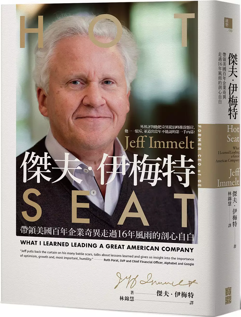
為了解決Electric cable 的問題,作者JeffImmelt 這樣論述:
美國百年企業前執行長首次公開完整自白, 闡述帶領奇異(GE)16年來的心路歷程 外界評判他把奇異從頂峰推落懸崖, 他一一駁斥,並供出當年那些不能說的第一手內幕! 甫上任三天就遇上911恐怖攻擊,隨後金融危機、311大地震更接二連三襲來。面對一個個重磅壞消息,傑夫.伊梅特如何力挽狂瀾,領軍奇異走過全球最動盪不安的歲月? 2001年9月11日,二架民航客機撞上世貿中心,改變了一切。在世界一瞬間陷入瘋狂、混亂之際,前一天才剛上任奇異執行長的傑夫.伊梅特冷靜分析現況、做出決策;儘管航空業備受衝擊,他仍下令在奇異航空投入更多資金,開發出後來裝進波音787夢幻客機(Dreamliner)的
GEnx引擎,也讓奇異航空的市占率在他任內成長了25%。 2004年,奇異股價陷入掙扎,他決定收購奇值金融、阿莫夏姆和NBC環球等不同產業。當年的媒體和分析師都痛批他的擴張太過魯莽,但這些決定的背後是根據他所秉持的組織原則,找出下一個趨勢後投資技術,最終得以賣到全世界並贏下市場。 2005年,為了因應客戶需求與大環境改變(經濟、環保、科學、技術),他推出「綠色想像」(Ecomagination),不只遭到內部極大反彈,更衝擊奇異其他能源生意,但也因此改變外界對奇異汙染環境的形象,環保新產品更創造2700億美元的營收。 2008年雷曼兄弟破產,美國經濟有如自由落體、全球金融崩盤
,他和團隊發行商業本票、找股神巴菲特增資,以挺過那段種種非比尋常事件襲來的日子。但有心人卻不時散播奇異情況不妙的謠言,試圖製造恐慌。 2010年,他成立「全球成長組織」(Global Growth Organization, GGO),期望奇異能成為具競爭力的公司,將業務拓展至全世界,卻也讓那些只想安坐在美國總公司的高層擔心權力被削弱,所以拚命地在背後扯他後腿。 2011年,他推動奇異數位(GE Digital)打造出工業分析平臺Predix。從現在的角度看來是一項極富市場價值和趨勢的產業,在當年卻被批評是一個沒有產出、燒錢速度卻極快的事業體,更無法快速複製奇異傳統的成功模式。
2015年,當全球趨勢走向綠能的時候,外界對於他大力支持收購法國阿爾斯通(Alstom)電力公司感到不諒解。但對他而言,是期望在收購這項傳統能源產業後,能幫助奇異電力在發展離岸風電等減少碳排放的再生能源上更加如虎添翼。 擔任奇異執行長的16個年頭,恐怖攻擊、金融危機、國際能源價格動盪和政治動亂等外部重大危機接踵而來,公司內部推動改革的腳步又太過緩慢,使他的計畫永遠趕不上變化。所以面對這些困境,他只能想辦法見招拆招,做出雖然不完美,但好過怕被指責而裹足不前的決定。 身處高位的人勢必飽受檢視和質疑,所以伊梅特用自身經驗說明他如何捱過最嚴厲尖銳批評:當下虛心接受但不予回應,只把心力放
在團隊經營和營運目標上。待卸下職位後,才回頭一一還原當年批評聲浪中,他只能做不能說、檯面下的決策考量。 這家擁有百年歷史的巨型企業如何走到今天這一步?傑夫.伊梅特真如外界所言是重挫奇異士氣的罪魁禍首,還是他所做的一切才是體現一個變動時代下新領導者的格局?沒有人會在領導者上任第一天給他一本手冊,教他如何解決棘手問題。所以身為領導者,當不可預期的危機來臨時,要如何不後悔地度過每一個做出重大決策的關鍵時刻? 「如果你既不是天才也不幸運,那我的故事對你就有參考價值。」 本書特色 1.由奇異前任執行長傑夫.伊梅特親自撰述,為最新、最完整且不假他人的第一手的資料。以第一人稱口吻敘述在奇
異擔任執行長的16個年頭中,經歷美國911事件、金融危機等衝擊,如何一路挺過這些困境做最詳實且赤裸的闡述。 2.透過作者身處其位的記實,讓讀者能一窺奇異大公司的營運方式,更能滿足對傑夫.伊梅特領導奇異期間感興趣的讀者。 重磅推薦 王文靜/品味私塾創辦人 鍾子偉/關鍵評論網執行長暨共同創辦人 ——依姓氏筆畫排序—— 對本書的讚譽 「兼具犀利洞察與真誠的非凡之作。傑夫・伊梅特在九一一前夕坐上奇異執行長位子,帶領這家指標性巨擘開啟叫人目眩神迷、常常動盪不安的十六年,這本書帶領讀者深入伊梅特的辦公室、腦袋和內心。這是一本必備手冊,教你領導,也教你人生。」——史坦利.A.麥
克里斯特爾(Stanley A. McChrystal)/美國陸軍上將(已退役)、McChrystal Group執行長兼創辦人 「傑夫・伊梅特一直是我在領導方面的榜樣。他用頭腦和心在領導,是一位『全心付出』的領導人,對團隊和客戶全心奉獻、關心。從這本書可看出,領導根本就是一種肉搏運動,傑夫在場上用盡全力,毫無保留。」——約翰.杜納霍(John Donahoe)/Nike執行長 「《傑夫・伊梅特》是對傑夫・伊梅特十六年奇異執行長生涯最權威、最私密的敘述。透過可貴的誠實與自覺,傑夫娓娓道出上百則引人入勝的故事,無私分享得來不易的領導教訓。《傑夫・伊梅特》是一則精彩、快節奏、紮紮實實的
愛情故事,傑夫個人對家庭和奇異人的愛,表露無遺,他對奇異真的是血淚付出(請見刺青一節)。如果你從事科技、金融、能源、醫療,這本書非讀不可,如果你關心世界大事、全球進展、公共服務,這本書深具啟發性。《傑夫・伊梅特》是一份大禮,來自傑夫這位個人英雄、愛國又了不起的僕人式領導人。」——約翰.多爾(John Doerr)/凱鵬華盈(Kleiner Perkins)創投董事長,著有《OKR:做最重要的事》(Measure What Matters) 「引人入勝的記錄,詳述在快速變動年代帶領一家跨國巨擘的種種戲劇性事件,領導教訓貫穿全書,是今日與未來的跨國商業領導人重要的讀物。」——鮑勃.達德利(B
ob Dudley)/英國石油公司(BP)前任執行長 「如果你的工作有過失敗或心碎(應該每個人都有過吧),傑夫這則充滿洞見、智慧、毅力、感情的故事,是寶貴的資源和藍圖,可供你借鏡參考去面對領導方面種種精彩的混亂。」——珍妮佛.阿克(Jennifer Aaker)/史丹佛商學院教授,著有《幽默,認真》(Humor, Seriously)一書 「傑夫・伊梅特為十六年奇異執行長生涯做了一番真誠坦率的回顧,剖析自己的成功與失敗,從當事人的視角說明他最受爭議的決策。他也探討了這份最孤獨、最具挑戰性的職位在情感和智力方面的挑戰,從中可獲得很多教訓。這是一個洞察犀利的視角,對當前與未來有抱負的領
導人都極具參考價值。」——托比.科斯格羅夫(Toby Cosgrove)/克里夫蘭醫學中心(Cleveland Clinic)執行顧問、前任總裁與執行長 「傑夫撕開了他身上的戰鬥傷疤,細數他所學到的教訓,讓我們瞭解樂觀、成長、謙卑的重要性。」——露絲.波拉特(Ruth Porat)/Alphabet與Google資深副總兼財務長 「傑夫用他執掌奇異超過十六年的智慧、自省、大膽領導,給奇異一段不凡的變革成長提出最具洞察力的觀點。這本書是最權威的描述,可一探當時發生的種種是如何開展。」——傑夫・畢帝(Geoff Beattie)/世代資本(Generation Capital)董事長兼
執行長 「《傑夫・伊梅特》是一本誠實勇敢的書,很少執行長的著作是如此。傑夫展現深深的謙遜,把讀者帶進奇異史上(也是美國史上)一段不尋常時期的董事會。書裡的犀利洞見是得自一段大起大落的事業生涯,傑夫絲毫不閃躲迴避。任何執行長、有抱負的商業主管、有團隊(不論大小)需要管理的人,都應該一讀。」——傑夫・札克(Jeff Zucker)/有線電視新聞網(Cable News Network, CNN)總裁 「《傑夫・伊梅特》提供了詳盡的細節,可以一窺帶領一家二十世紀最成功的多角化工業公司進入動盪的二十一世紀所面臨的劇烈挑戰。從這本書可以看出,需要多麽龐大的精力、熱情和投入,才能巡航於高度複雜
且全球化的商場上。透過書中種種難以置信事件及商業投資的挑戰,傑夫充沛的精力及富有魅力的領導風格一覽無遺,還有他對創新、客戶、員工堅定不移的承諾。此外,《傑夫・伊梅特》也提供了許多洞察犀利的商業領導經驗。」——約瑟夫・霍根(Joseph M. Hogan)/愛齊科技(Align Technology)總裁兼執行長 「《傑夫・伊梅特》是一本有意思、吸引人的書。書中記錄了傑夫・伊梅特在奇異的事業發展、他的時間都花在哪些事務上(尤其在執行長任內)、他自己的成長以及他如何培養他人。針對他所做的許多關鍵決策(挑選領導人、買賣公司、投資哪些事業與不投資哪些事業),這本書也提供了背景說明和觀察視角。就像
其他大企業一樣,他的決策有人認同也有人不認同,但是他清楚說明了箇中緣由。特別有價值且發人深省的是其中的商業領導經驗,任何人都能從這本書獲益匪淺。我強烈推薦。」——奧馬爾・伊什拉克(Omar Ishrak)/曾任美敦力醫療(Medtronic)執行長、董事長 「衡量一本商業領導書籍好不好,要看有多少內容會讓你為了日後參考而畫線做記號,我在《傑夫・伊梅特》畫了一百九十二處。如果你要的是『看看我多麽厲害』的回憶錄,那這本書就別考慮了,如果你要的是真正的教訓,帶領全球最複雜企業度過全球最具挑戰、最不可預測的十六年所獲得的真正教訓,那就找個位子坐下來翻開第一頁。」——安德魯・羅伯遜(Andrew
Robertson)/BBDO全球廣告(BBDO Worldwide)總裁兼執行長 「讀完這本書,你會成為更好的領導人。」——大衛・羅吉爾(David Rogier)/MasterClass線上學習平臺創辦人兼執行長 「在這本敘述精妙的傳記中,傑夫・伊梅特給正在打造跨國企業的執行長上了一堂大師課,因為現今的執行長正在遭逢前所未有的變化和極端風險。這本書的讀者等於是打開了一扇罕有的窗戶,一窺關鍵時刻的領導是多麽孤獨,並且學到及時且永不過時的領導教訓。從這本書可以學到如何更有效地經營公司,如何成為更好的人,所以這不只是一本必讀的書,更是一本隨時都有參考價值的書。」——K. R. 斯里達
爾(K. R. Sridhar)/Bloom Energy創辦人兼執行長
基於石墨烯及生物碳基材料的可撓式電晶體應用與能量攫取
為了解決Electric cable 的問題,作者Mamina Sahoo 這樣論述:
Table of ContentsAbstract.......................................................................................................iFigure Captions........................................................................................xiTable Captions...................................................
....................................xxiChapter 1: Introduction1.1 Flexible electronics................................................................................11.2 Graphene the magical material ………………………….……….......21.2.1 Synthesis of graphene…………………………….….…...21.2.1.1 Mechanical exfoliati
on of graphene………………...……21.2.1.2 Epitaxial growth on Sic substrate………………….…..31.2.1.3 Chemical vapor deposition (CVD) method………….…..41.2.2 Graphene transfer…………………………………………....41.3 Application of graphene based Electronics……………………….......51.3.1 Graphene based flexible transparent electrode
……………….61.3.2 Top gated Graphene field effect transistor…………………….71.4 Challenges of flexible graphene based field effect transistors.……….91.5 Energy harvesting devices for flexible electronics………….........….91.6 Solar cell…………………………………………………………...101.6.1 Device architecture…………………………………………101.
6.2 Issues and Challenges of Perovskite solar cells………...121.7 Triboelectric nanogenerator (TENG)………………………………121.7.1 Working mode of TENG………………………………….141.8 Applications of TENG………………………………………………151.8.1 Applications of graphene based TENG…………………....151.8.2 Applications of bio-waste material ba
sed TENG………….171.9 Key challenges of triboelectric nanogenerator…………………....…191.10 Objective and scope of this study………………………………....19Chapter 2: Flexible graphene field effect transistor with fluorinated graphene as gate dielectric2.1 Introduction………………………………………………………....212.2 Material preparation a
nd Device fabrication………………. 232.2.1CVD Growth of Graphene on Copper Foil………………….232.2.2 Transfer of graphene over PET substrate……………...........252.2.3 Fabrication of fluorinated graphene ……………...........252.2.4 F-GFETs with FG as gate dielectric device fabrication……262.2.5 Material and electrical C
haracterization …………………272.3 Results and discussion…………………………………………….282.3.1 Material characterization of PG and FG……………...…...….282.3.2 Electrical characterization of F-GFET with FG as dielectrics..332.3.3 Mechanical stability test of F-GFET with FG as dielectrics ….362.4 Summary…………………………………………………
………....40Chapter 3: Robust sandwiched fluorinated graphene for highly reliable flexible electronics3.1 Introduction………………………………………………………….423.2 Material preparation and Device fabrication ………………….........443.2.1 CVD Growth of Graphene on Copper Foil…………………...443.2.2 Graphene fluorination …...…….…………
…………..............443.2.3 F-GFETs with sandwiched FG device fabrication....................443.2.4 Material and electrical Characterization…..............................453.3 Results and discussion ……………………………………...............453.3.1 Material characterization of sandwiched…………………….453.3.2 Electric
al characterization of F-GFET with sandwiched FG....473.3.3 Mechanical stability test of F-GFET with sandwiched FG…503.3.4 Strain transfer mechanism of sandwiched FG………………513.4 Summary…………………………………………………………....53Chapter 4: Functionalized fluorinated graphene as a novel hole transporting layer for ef
ficient inverted perovskite solar cells4.1 Introduction………………………………………………………….544.2 Material preparation and Device fabrication......................................564.2.1 Materials ………………………...…………………………564.2.2 CVD-Graphene growth ……………………………...…...564.2.3 Graphene fluorination …………………………………….564.
2.4 Transfer of fluorinated graphene…………………………...574.2.5 Device fabrication …………………………………….….574.2.6 Material and electrical Characterization …….....................584.3 Results and discussion …………………………………………….594.3.1 Surface electronic and optical properties of FGr……….….594.3.2 Characterization o
f FGr and perovskite surface ……….…644.3.3 Electrical performance of PSC………………….…….…...694.3.4 Electrical performance of Flexible PSC……………………724.4 Summary…………………………………………………………...78Chapter 5: Flexible layered-graphene charge modulation for highly stable triboelectric nanogenerator5.1 Introduction…………
…………………………………………....795.2 Experimental Section……………………………………………….825.2.1 Large-area graphene growth ……………………………….825.2.2 Fabrication of Al2O3 as the CTL …………………………...825.2.3 Fabrication of a Gr-TENG with Al2O3 as the CTL………825.2.4 Material characterization and electrical measurements…….835.3 Results
and discussion.…………………………………...…………845.3.1 Material Characterization of Graphene Layers/Al2O3……845.3.2 Working Mechanism of Gr-TENG with Al2O3 as CTL…915.3.3 Electrical Characterization of Gr-TENG with Al2O3 CTL…945.3.4 Applications of the Gr-TENG with Al2O3 as CTL……….1015.4 Summary…………………………………………
……………….103Chapter 6: Eco-friendly Spent coffee ground bio-TENG for high performance flexible energy harvester6.1 Introduction…………………………………………………….......1046.2 Experimental Section…………………………………………….1086.2.1 Material Preparation …………………………………….1086.2.2 Fabrication of SCG powder based TENG………………...1086
.2.3 Fabrication of SCG thin-film based TENG ………………1096.2.4 Material characterization and electrical measurements….1106.3 Results and discussion.…………………………………...………1116.3.1 Material Characterization of SCG powder and thin film….1116.3.2 Working Mechanism of SCG-TENG……………………...1186.3.3 Electrical Cha
racterization of SCG-TENG……………….1226.3.4 Applications of the SCG thin-film based TENG………….1326.4 Summary………………………………………………………….134Chapter 7: Conclusions and future perspectives7.1 Conclusion………………………………………………………....1357.2 Future work …………………………….………………………….1377.2.1 Overview of flexible fluorinated g
raphene TENG..............1377.2.1.1 Initial results………………………………….…1387.2.2.1.1 Fabrication of FG-TENG………………1387.2.2.1.2 Working principle of FG-TENG……….1397.2.2.1.3 Electrical output of FG-TENG.………...140References…………………………………………………………….142Appendix A: List of publications………………….……………..........177A
ppendix B: Fabrication process of GFETs with fluorinated graphene (FG) as gate dielectric……........……………………………………….179Appendix C: Fabrication process of GFETs with sandwiched FG…....180Appendix D: Fabrication process of inverted perovskite solar cell with FGr as HTL…………………………………………………………….181Appendi
x E: Fabrication of a Gr-TENG with Al2O3 as the CTL…….182Appendix F: Fabrication of SCG based triboelectric nanogenerator….183Figure captionsFigure 1-1 Exfoliated graphene on SiO2/Si wafer……………………….3Figure 1-2 Epitaxial graphene growth on SiC substrate………………....3Figure 1-3 Growth mechanism of graphe
ne on Cu foil by CVD ……......4Figure 1-4 Wet transfer process of CVD grown graphene…………...….5Figure 1-5 RGO/PET based electrodes as a flexible touch screen.……....6Figure 1-6 Graphene based (a) touch panel (b) touch-screen phone…….7Figure 1-7 Flexible graphene transistors (a) (Top) Optical photograph
of an array of flexible, self-aligned GFETs on PET. (Bottom) The corresponding schematic shows a device layout. (b) Schematic cross-sectional and top views of top-gated graphene flake–based gigahertz transistors. (Left) AFM image of a graphene flake. (Right) Photograph of flexible graphene devices
fabricated on a PI substrate. (c) Cross-sectional schematic of flexible GFETs fabricated using a self-aligned process……8Figure 1-8 The magnitude of power needed for meet certain operation depending critically on the scale and applications………………………10Figure 1-9 Schematic diagrams of PSC in the (a) n-i
-p mesoscopic, (b) n-i-p planar, (c) p-i-n planar, and (d) p-i-n mesoscopic structures………...12Figure 1-10 Schematic illustration of the first TENG...………………...13Figure 1-11 Working modes of the TENG. (a) The vertical contact-separation mode. (b) The lateral sliding mode. (c) The single-electrode mode
. (d) The free-standing mode ………………………………...……14Figure 1-12 Schematic illustration of (a) device fabrication of graphene-based TENGs (b) graphene/EVA/PET-based triboelectric nanogenerators (c) device fabrication of stretchable CG based TENG with electrical output performance……………………………………………………...17
Figure 1-13 Schematic illustration and output performance of bio-waste material based TENG (a) Rice-husk (b) Tea leaves (c) Sun flower powder (SFP) (d) Wheat stalk based TENG………….…………………………18Figure 2-1 Graphene synthesis by LPCVD method……….…………...24Figure 2-2 Schematic diagram of (a) preparation pro
cess of 1L-FG/copper foil (b) Layer by layer assembly method was used for fabricating three-layer graphene over copper foil and then CF4 plasma treatment from top side to form 3L-FG/copper foil…………………….26Figure 2-3 Schematic illustration of fabrication process of F-GFET with FG as gate dielectric ……
……………………………………………….27Figure 2-4 (a) Raman spectra of PG, 1L-FG and 3L-FG after 30 min of CF4 plasma treatment over copper foil. (b) Peak intensities ratio ID/IG and optical transmittance of PG, 1L-FG and 3L-FG. Inset: image of PG and 1L-FG film over PET substrate. (c) Typical Raman spectra of PG, 1L
-FG and 3L-FG on PET substrate. (d) Optical transmittance of PG, 1L-FG and 3L-FG film over PET substrate. The inset shows the optical image of GFETs with FG as gate dielectrics on PET ……….…………30Figure 2-5 XPS analysis result of (a) PG (b) 1L-FG (c) 3L-FG where the C1s core level and several carbon f
luorine components are labeled. The inset shows the fluorine peak (F 1s) at 688.5 eV……………………….32Figure 2-6 (a) Water contact angle of PG, 1L-FG and 3L-FG over PET substrate. (b) The relationship between water contact angle of PG, 1L-FG and 3L-FG and surface-roughness………………………………………33Figure 2-7 (a) I
d vs. Vd of w/o-FG, w/1L-FG and w/3L-FG samples after 30 min of CF4 plasma (b) Id vs. Vg of w/o-FG, w/1L-FG and w/3L-FG samples at a fixed value of drain to source voltage, Vds of 0.5 V (c) Gate capacitance of w/o-FG, w/1L-FG and w/3L-FG samples (d) Gate leakage current of w/o-FG (naturally formed A
l2OX as gate dielectric), w/1L-FG and w/3L-FG samples ……………………………...…………...……...34Figure 2-8 (a) Schematic illustration of bending measurement setup at different bending radius. (i) Device measurement at (i) flat condition (ii) bending radius of 10 mm (iii) 8 mm (iv) 6 mm. Inset shows the photograph
of measurement setup. Change in (b) carrier mobility (c) ION of w/o-FG, w/1L-FG and w/3L-FG samples as a function of bending radius. The symbol ∞ represents the flat condition. Change in (d) carrier mobility (e) ION of w/o-FG, w/1L-FG and w/3L-FG samples as a function of bending cycles (Strain = 1.
56%)…………………………………….38Figure 3-1 Schematic illustration of the flexible top gate graphene field effect transistor with sandwich fluorinated graphene (FG as gate dielectric and substrate passivation layer) ……………………………...…………44Figure 3-2 Raman spectra of (a) PG/PET and PG/FG/PET substrate (b) sandwiche
d FG (FG/PG/FG/PET). Inset showing the optical transmittance of sandwiched FG. (c) HRTEM image for 1L-FG.……………….….…46Figure 3-3 (a) Id vs. Vd of FG/PG/FG device at variable vg (−2 to 2 V). (b) Id vs. Vg of FG/PG/FG. (c) Gate capacitance of FG/PG/FG ….…….48Figure 3-4 Raman spectra of devices under be
nding (a) PG/PET (Inset shows the 2D peak) (b) PG/FG/PET (inset shows the 2D peak) …….…49Figure 3-5 (a) Change in Mobility (b) change in ION of PG/PET and PG/FG/PET as a function of bending radius between bending radii of ∞ to 1.6 mm in tensile mode (c) Change in Mobility (d) Change in ION of PG/PET
and PG/FG/PET as a function of bending cycles. Inset of (c) shows the photograph of F-GFETs with sandwich FG on the PET substrate (e) change in resistance of w/1L-FG, 1L-FG/PG/1L-FG samples as a function of bending radius ………………………...……………….50Figure 3-6 Schematic evolution of proposed strain transf
er mechanism through PG/PET and PG/FG/PET. The inset of PG/PET sample shows the generation of sliding charge due to interfacial sliding between PG and PET ………………………………………………………………….….52Figure 4-1 FGr fabrication and transfer process …………….………....57Figure 4-2 (a) Raman analysis of pristine graphene a
nd the FGr samples after 5, 10, 20, and 30 min of CF4 plasma treatment over Cu foil (b) Raman intensity ratios (I2D/IG and ID/IG) of fluorinated graphene, with respect to the exposure time ……………………………………………60Figure 4-3 SEM images of (a) ITO, (b) ITO/1L-FGr, (c) ITO/2L-FGr, and (d) ITO/3L-FGr …………………
………………………………….61Figure 4-4 XPS analysis of FGr with (a) 5 min (b) 10 min and (c) 20 min of CF4 plasma treatment on the Cu foil (d) The fluorine peak (F1s) of FGr (f) The correlation of the carbon-to-fluorine fraction (C/F) with exposure time and the corresponding carrier concentrations …………….………62Fi
gure 4-5 Tauc plots and UV–Vis absorption spectra of FGr films with CF4 plasma treatment for (a) 5, (b) 10, and (c) 20 min ….………......….63Figure 4-6 WCAs on PEDOT: PSS and 1L, 2L, and 3L FGr samples ...64Figure 4-7 (a) Mechanism of large grain growth of perovskite on a non-wetting surface (b) Top-vi
ew and cross-sectional surface morphologies of perovskites on various HTLs ………………………………...…………65Figure 4-8 XRD of perovskite films on various HTL substrates ….…...66Figure 4-9 UPS spectra of various numbers of FGr layers on ITO: (a) cut-off and (b) valance band spectra …………………………………….….67Figure 4-10
Energy band diagrams of PSCs with (a) PEDOT: PSS, (b) 1L-FGr, (c) 2L-FGr, and (d) 3L-FGr as HTL …………………….…….68Figure 4-11 (a) Steady state PL spectra of PEDOT: PSS/perovskite and FGr/perovskite films. (b) TRPL spectral decay of PEDOT: PSS/perovskite and FGr/perovskite films………………………….……69Figure 4-1
2 (a) Schematic representation of a PSC having an inverted device configuration. (b) Cross-sectional HRTEM image of the ITO/ FGr–perovskite interface………………………………………...………70Figure 4-13 Photovoltaic parameters of PSCs incorporating various HTL substrates: (a) PCE (%), (b) Voc (V), (c) Jsc (mA/cm2), an
d (d) FF (%)....71Figure 4-14 Normalized PCEs of target and control PSCs incorporating various HTL substrates, measured in a N2-filled glove box. (a) Thermal stability at 60 °C (b) Light soaking effect under 1 Sun (c) Stability after several days …………………………………………………………….72Figure 4-15 (a) Schematic r
epresentation of the structure of a flexible PSC on a PET substrate (b) J–V curves of control and target flexible PSCs, measured under both forward and reverse biases. (c) Average PCE of flexible PSCs incorporating PEDOT: PSS and FGr HTLs……….…73Figure 4-16 (a) Normalized averaged PCEs of the flexibl
e PSCs after bending for 10 cycles at various bending radii. (b) Normalized averaged PCEs of the flexible PSCs plotted with respect to the number of bending cycles at a radius of 6 mm ………………………………………………75Figure 4-17 Photovoltaics parameters of flexible PSCs with various HTL substrates: (a) JSC (mA/c
m2), (b) Voc (V), and (c) FF (%) ……………....75Figure 4-18 XRD patterns of perovskite films on PET/ITO/FGr, recorded before and after bending 500 times …………………………………….76Figure 4-19 SEM images of (a) perovskite films/FGr/ITO/PET before bending (b) after bending 500 times (c) perovskite films/PEDOT: PSS/
ITO/PET before bending (d) after bending 500 times ……………….…77Figure 4-20 PL spectra of perovskite films on PET/ITO/FGr, recorded before and after various bending cycles …………………………….…78Figure 5-1 Schematic illustration showing the fabrication process of a flexible Gr-TENG with Al2O3 as the CTL ……………
………………...83Figure 5-2 The Raman spectra of (a) graphene/Al-foil/PET and (b) graphene/Al2O3/Al-foil/PET. The I2D/IG of graphene layers (1L, 3L and 5L) over (c) Al-foil/PET substrate (d) Al2O3/Al-foil/PET substrate …...85Figure 5-3 XRD patterns of (a) graphene/Al-foil/PET and (b) graphene/Al2O3/Al-foi
l/PET ……………………………………………86Figure 5-4 FESEM image of the graphene surface on (a) Al-foil/PET and (b) Al2O3/Al-foil/PET. EDS analysis of (c) graphene/Al-foil/PET and (d) graphene/Al2O3/Al-foil/PET (e) EDS elemental mapping of the graphene/Al2O3/Al-foil/PET presenting C K series, O K series and Al K ser
ies …………………………………………………………….………87Figure 5-5 3D AFM images of (a) 1L-Gr (b) 3L-Gr (c) 5L-Gr on Al foil (d) 1L-Gr (e) 3L-Gr (f) 5L-Gr on Al2O3/Al foil………………….….….89Figure 5-6 Work function of graphene layers on the (a) Al-foil (b) Al2O3/Al-foil substrate by KPFM. Inset showing the surface potential of
graphene layers (1L, 3L and 5L) over Al-foil and Al2O3 substrate (c) energy band diagrams for 1L-Gr, 3L-Gr and 5L-Gr over Al2O3 ……....90Figure 5-7 Schematic illustration of Electronic energy levels of graphene samples and AFM tip without and with electrical contact for three cases: (i) tip and the
1L-Gr (ii) tip and the 3L-Gr and (iii) tip and the 5L-Gr over Al2O3/Al foil/PET……………………………………….…...…………91Figure 5-8 Working mechanism of Gr-TENG with Al2O3 ….….…...…93Figure 5-9 a) ISC and (b) VOC of 1L-, 3L- and 5L-Gr-TENGs without Al2O3 CTL (c) Sheet resistance of graphene as a function of number
of layers ………………………………...…...…………………………….95Figure 5-10 Electrical output of the Gr-TENG with Al2O3 CTL: (a) ISC and (b) VOC of 1L-, 3L- and 5L-Gr. Magnification of the (c) ISC and (d) VOC of the 3L-Gr-TENG with Al2O3 as the CTL. Average mean (e) ISC and (f) VOC generated by pristine Gr-TENGs (1L, 3L
and 5L) and Gr-TENGs (1L, 3L and 5L) with Al2O3 CTL. Error bars indicate standard deviations for 4 sets of data points ……………...…………….….…......96Figure 5-11 (a) CV of Al/Al2O3/3L-Gr/Al at 100 kHz and 1 MHz (b) CV hysteresis of 3L-Gr-TENG with Al2O3 as CTL with different sweeping voltages (c) Surface
charge density of graphene (1L, 3L and 5L)-based TENG with and without Al2O3 as CTL ………………………………...98Figure 5-12 Circuit diagram of output (a) VOC and (b) ISC measurement of 3L-Gr TENG with Al2O3 CTL as a function of different resistors as external loads. Variation in VOC and ISC w.r.t different re
sistors as external loads of (c) 3L-Gr TENG with Al2O3 CTL (d) 3L-Gr TENG without Al2O3 CTL. Relationship between electrical output power and external loading resistance (e) 3L-Gr TENG with Al2O3 CTL (f) 3L-Gr TENG without Al2O3 CTL…………………………………….………………...99Figure 5-13 (a)Electrical stability and du
rability of the 3L-Gr TENG with Al2O3 (b) Schematic illustrations showing the charge-trapping mechanism of 3L-Gr-TENG without and with Al2O3 charge trapping layer ………101Figure 5-14 (a) Photograph showing 20 LEDs being powered (b) Circuit diagram of bridge rectifier (c) Charging curves of capacitors
with various capacitances (d) Photograph of powering a timer …….………………102Figure 6-1 The schematic diagram of the fabrication process for SCG powder based TENG ……………………………………………….….108Figure 6-2 The schematic diagram of the fabrication process for SCG thin-film based TENG via thermal evaporation meth
od ………………109Figure 6-3 FESEM image of (a) SCG powder (inset image illustrates the high magnification of SCG powder) (b) SCG thin-film/Al foil/PET (inset image illustrates the high magnification of SCG thin-film). EDS of the (c) SCG powder (d) SCG thin-film/Al foil/PET…………………………. 112Figure 6-4 Raman
spectra analysis (a) pristine SCG powder (b) SCG thin-film/Al foil/PET. XRD patterns of (c) SCG powder (d) SCG thin film with different thickness ……………………………………… ……….115Figure 6-5 FTIR analysis of the (a) pristine SCG powder sample (b) SCG thin film………………………………………………………………...116Figure 6-6 3D AFM ima
ge of SCG thin-film with various thickness (a) 50 nm (b)100 nm and (c) 200 nm……………………………………...117Figure 6-7 Schematic illustration of working principle of SCG thin-film based TENG …………………………………………………………...119Figure 6-8 Finite element simulation of the generated voltage difference for SCG thin-film b
ased TENG based on the contact and separation between SCG thin film and PTFE …………….……………………….120Figure 6-9 (a) The setup for electrical property testing, which including a Keithley 6514 system electrometer and linear motor. Electrical output (b) ISC (c) VOC of TENGs based on different friction pairs
for checking the triboelectric polarity of SCG…………………………………………...123Figure 6-10 Electrical measurement of (a) ISC and (b) VOC of the SCG thin-film based TENG. Mean value of (d) ISC (e) VOC and (f) Output power density of the pristine SCG powder and thermal deposited SCG thin-film based TENG. ...………
………………………………………125Figure 6-11 (a) Schematic illustration of KPFM for measuring the work function. (b) Surface potential images of SCG thin film with various thickness (50 nm, 100 nm and 200 nm). (c) Surface potential and (d) Work function vs SCG thin film with various thickness (50 nm, 100 nm and 20
0 nm).………….……………………………………………….128Figure 6-12 (a) Isc and (b) Voc of SCG thin film based TENG under different contact frequencies (c) Isc and (d) Voc of SCG thin film based TENG under different separation distance…………………………….129Figure 6-13 Electrical response (a) ISC (b) VOC of pristine SCG powder an
d (c) ISC (d) VOC of SCG thin-film based TENG with respect to different relative humidity (35-85% RH) …………………………….131Figure 6-14 Electrical stability and durability test of the output performance of (a) pristine SCG powder based TENG (b) SCG thin-film based TENG……………………………………………………………132Figure 6-15
Applications of the SCG thin film based TENG as a power supply: (a) Circuit diagram of the bridge-rectifier for charging a capacitor (b) Charging curves of capacitors with various capacitances (0.1, 2.2 and 3.3 µF) (c) Photograph of powering a timer…………………...………133Figure 7-1 Schematic illustration o
f FG based TENG…….….……….139Figure 7-2 Working mechanism of FG based TENG…………………140Figure 7-3 Electrical output of FG-TENG: (a) Isc and (b) Voc …….….141Table captionsTable 2-1 Comparison of flexible G-FETs on/off ratio of our work with other’s work…………………………………………………...………...40Table 3-1 Summary of th
e electrical and mechanical performance of flexible w/o-FG, w/ 1L-FG, w/3L-FG and sandwich FG (FG/PG/FG) samples......................................................................................................52Table 3.2: Comparison of the electrical and mechanical performance of sandwich FG ba
sed F-GFET with previous F-GFET with different gate dielectrics……………………………………………………….………53Table 4-1 Best photovoltaic performance from control and target devices prepared on rigid and flexible substrates……………………………......74Table 5-1 EDS elemental analysis of graphene over Al-foil/PET and Al2O3/Al-foi
l/PET ………………………………………………………88Table 5-2 Comparison of electrical output performance of Gr-TENGs with and without Al2O3 CTL samples used in this study………………103Table 6-1 EDS elemental analysis of SCG-Powder and SCG thin film /Al foil/PET………………………………………………………………...113Table 6-2 Comparison of electrical o
utput performance of SCG-TENGs samples used in this study……………………………………………...126